| |
|
|
 |
|
 |
Silicon
Usually we are handling Silicon monocrystalline, CZ and
FZ, optical and mirror grade.
Silicon (Si) is grown by
Czochralski pulling techniques (CZ) and contains some oxygen that
causes an absorption band at 9 microns. To avoid this, material can
be prepared by a Float-Zone (FZ) process. Optical silicon is
generally lightly doped (5 to 40 ohm cm) for best transmission above
10 microns, and doping is usually boron (p-type) and phosphorus
(n-type). After doping silicon has a further pass band: 30 to 100
microns which is effective only in very high resistivity
uncompensated material.
CZ Silicon is commonly used as substrate
material for infrared reflectors and windows in the 1.5 - 8 micron
region. The strong absorption band at 9 microns makes it unsuitable
for CO2 laser transmission applications, but it is frequently used
for laser mirrors because of its high thermal conductivity and low
density. Application as window, lens in the 1.5 - 8 μm region;
Mirror for CO2 laser and spectrometer applications.
Si Mirror
grade
Any dopant, any conductivity, any orientation, not
warranted with respect to transmission, suitable for mirror
substrates.
Si Optical grade
CZ, P type doped with Boron,
<111> or <100>, Resistivity 5 - 40 ohmcm
FZ, N type
doped with Phosphorus, <111>, Resistivity > 50, preferably
> 500 ohmcm, the absorption at 9 microns is absent.
Also we
produced Silicon wafers according customers specifications, these
substrates can be used in the semiconductor production.
We can
offer services like lapping, cutting, grinding, polishing,
double-side polishing.
Main Properties
Crystal properties |
Crystal Growth Method |
Czohralski (CZ) & Floatzone (FZ) |
Max. Size (mm)
CZ
FZ |
< F350mm
< F125mm |
Optical properties |
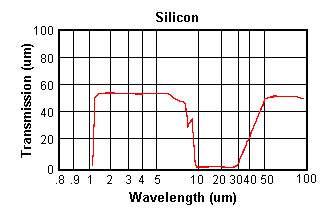
Transmission Range |
1.2~8um |
Reflection Loss, for two surfaces at 5 um |
46.2% |
Refractive Index |
See below |
Wavelength (um) |
Refractive Index (n) |
Wavelength (um) |
Refractive Index (n) |
1.357 |
/ |
5.500 |
3.4213 |
1.3951 |
3.4975 |
6.000 |
3.4202 |
1.6606 |
3.4929 |
6.500 |
3.4195 |
1.8131 |
3.4608 |
7.000 |
3.4189 |
2.1526 |
3.4476 |
7.500 |
3.4186 |
2.3254 |
3.443 |
8.000 |
3.4184 |
3.000 |
3.432 |
8.500 |
3.4182 |
3.500 |
3.4284 |
10.00 |
3.4179 |
4.000 |
3.4257 |
10.50 |
3.4178 |
4.500 |
3.4236 |
11.04 |
3.4176 |
5.000 |
3.4223 |
|
|
Transmission Curve |
See below |
|
Crystallographic properties |
Syngony |
Cubic |
Lattice Constant, Angstrom (Å) |
5.43 |
Physical properties |
Density |
2.33g/cm3 |
Hardness, Mohs |
7 |
Dielectric Constant for 9.37 x 10⁹ Hz |
13 |
Melting Point, °C |
1414 |
Thermal Conductivity, W/m・K at 313 K |
163 |
Thermal Expansion, 1/K at 293 K |
2.6x10⁻⁶ |
Specific Heat Capacity, J/(kg/°C) |
712.8 |
Bandgap, eV |
1.1 |
Knoop Hardness, kg/mm2 |
1100 |
Young's Modulus, Gpa |
130.91 |
Shear Modulus, GPan |
79.92 |
Bulk Modulus, GPa |
101.97 |
Debye Temperature, K |
640 |
Poisson's Ratio |
0.28 |
Chemical properties |
Solubility in water |
None |
Molecular Weight |
28.09 |
Silicon Products General Specifications:
Optical grade Silicon Window
Substrates |
Parameters |
Commercial Grade |
Precision Grade |
Substrate Material |
CZ or FZ optical Silicon mono |
Diameter Tolerance |
+0/-0.10mm |
Thickness Tolerance |
+/-0.10mm |
Clear Aperture |
>Central 90% of diameter |
Surface Quality |
60-40 S/D |
40-20 S/D |
Parallelism |
3~5 arc min |
1 arc min |
Surface Flatness |
1λ per 25mm |
λ/4 |
Chamfer |
0.15~0.35mmx45° face width x45+/-15° |
Coating |
Coatings are available upon
request |
Optical Grade Silicon Lens Substrates |
Parameters |
Commercial grade |
Precision grade |
Ultra-precision grade |
Substrate Material |
CZ or FZ optical Silicon mono |
Diameter Tolerance |
+0/-0.10mm |
Thickness Tolerance |
±0.10mm |
Focal Length Tolerance |
<±1% |
Clear Aperture |
>Central 90% of diameter |
Surface Quality |
60-40 S/D |
40-20 S/D |
20-10 S/D |
Centration |
<3 arc min |
<1 arc min |
Surface Flatness |
Power<3
fringes(1.5λ)
Irregularity<0.5 fringes(λ/4) |
Irregularity<0.2 fringes(λ/10) |
Chamfer |
0.15~0.35mm×45° face width × 45°±15° |
Coating |
Coatings are available upon request |
No coating |
Silicon Wafers |
Parameters |
Value |
Substrate Material |
CZ Silicon, N or P, R=0.003~50
ohm.cm |
Orientation |
<100> / <111> |
Diameter Tolerance |
3"~8"±0.2mm |
Thickness Tolerance |
According to SEMI or customer’s requirements
T±15um |
Thickness Vary (TTV) |
<5um |
Surface Flatness (TIR) |
<4um |
Surface (STIR) |
<0.6um |
Warp |
<30um |
|
|
|
|
|